What Replaced Vacuum Tubes? A Proven Guide for 2027
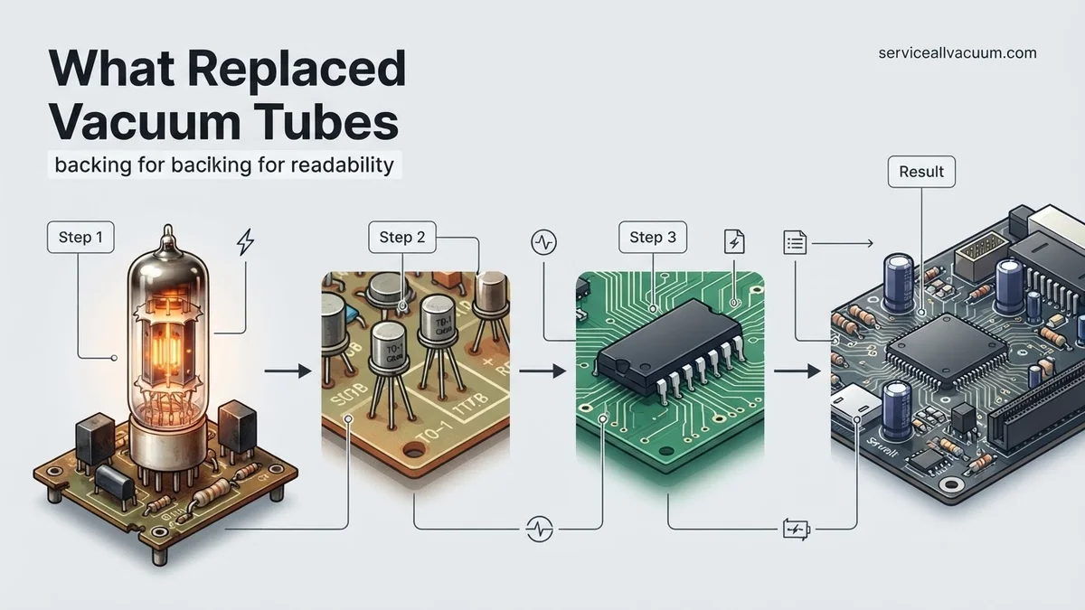
Transistors directly replaced vacuum tubes, revolutionizing electronics with their smaller size, lower power consumption, and greater reliability. This shift paved the way for modern computing and integrated circuits, fundamentally changing technology as we know it.
If you’re asking what truly revolutionized electronics and directly replaced the bulky, power-hungry vacuum tubes of yesteryear, the answer is unequivocally the transistor. This small, unassuming semiconductor device completely reshaped computing, communication, and virtually every piece of electronic equipment we interact with daily. Its evolution into integrated circuits is the bedrock of modern technology.
Understanding this transition isn’t just a historical curiosity; it’s crucial for appreciating the scale of innovation that enables your 2027 smartphone, the AI driving your smart home, and the vast cloud infrastructure that powers our digital world. Without the transistor, none of this would be possible. It allowed for the miniaturization and efficiency that defines our current tech landscape.
Key Takeaways
- Transistors were the primary replacement.
- Enjoyed smaller size, less power use.
- Integrated Circuits built on this foundation.
- Enabled massive electronic miniaturization.
- Underpins all modern digital devices.
What Caused the Need to Replace Vacuum Tubes?
The Era of Tubes and Their Inherent Limitations
Before the transistor, vacuum tubes were the workhorses of electronics, amplifying signals and switching currents in everything from radios to early computers. However, they came with significant drawbacks that severely limited technological progress. Imagine a computer made of thousands of light bulbs; that’s essentially what vacuum tubes were like. They were:
- Bulky and Heavy: Each tube was a glass envelope, often centimeters in size, making devices large and cumbersome.
- Fragile: Made of glass, they were susceptible to breakage from shock or vibration.
- Power Hungry: They required high voltages and significant power to heat a filament, like a light bulb, to operate.
- Heat Generators: All that power consumption led to excessive heat, which not only wasted energy but also shortened component lifespans and required elaborate cooling systems.
- Short Lifespan: Filaments would burn out, and the vacuum could degrade, necessitating frequent and costly replacements.
- Slow Switching: Their operational principles meant they couldn’t switch on and off as quickly as needed for truly high-speed processing.
The Practical Impact on Early Electronics
These limitations meant that early electronic devices were monumental undertakings. The famous ENIAC computer from the 1940s, for example, used over 17,000 vacuum tubes, weighed 30 tons, occupied 1,800 square feet, and consumed 150 kilowatts of power – enough to dim the lights in a small town when it was switched on. Imagine powering your 2027 AI servers with such components! Portable electronics were practically non-existent due to size, weight, and power demands. Maintenance was a constant headache, as tubes failed regularly, requiring technicians to hunt down the faulty component. This inherent unreliability and scale were massive roadblocks to widespread electronic adoption.
From Start to Finish: The Rise of Semiconductors Explained
This guide meticulously charts the revolutionary journey from bulky, power-hungry vacuum tubes to the ubiquitous, miniature marvels we know as semiconductors. Understanding this transition isn’t just about historical facts; it’s about grasping the fundamental innovation that powered the digital age, from the first computers to the smartphones in our pockets. Follow these steps to gain a comprehensive insight into the “what” and “how” behind this monumental technological shift.
Step 1: Understanding Vacuum Tube Limitations
What you need: A basic grasp of early electronics, awareness of physical constraints, and an appreciation for engineering challenges of the mid-20th century.
Instructions: Begin by envisioning the state of electronics prior to the semiconductor era. Vacuum tubes, specifically triodes, acted as switches and amplifiers by controlling electron flow in a vacuum. However, they were inherently large (think light bulbs), consumed significant power (generating considerable heat), were fragile (glass envelopes, delicate filaments), and had a limited lifespan, often failing after a few thousand hours. Projects like ENIAC, the first electronic general-purpose computer, famously used around 17,468 vacuum tubes, occupied 1,800 square feet, and weighed 30 tons, clearly illustrating their immense practical drawbacks.
Pro Tip: Consider the energy efficiency. A single vacuum tube might draw watts of power, whereas a modern transistor in a microprocessor might draw pico-watts. This difference isn’t just about size; it’s fundamental to mobile computing and battery life.
Step 2: The Birth of the Transistor
What you need: An interest in foundational scientific discoveries, knowledge of basic physics concepts (conduction, semiconductors), and an understanding of Bell Labs’ role in innovation.
Instructions: The quest for a smaller, more reliable alternative led to intensive research into semiconductor materials. In 1947, at Bell Telephone Laboratories, John Bardeen, Walter Brattain, and William Shockley made a monumental breakthrough: the invention of the point-contact transistor. Their device, composed of a germanium crystal and two gold point contacts, demonstrated amplification. This marked the very first time a solid-state device could perform the same electronic functions as a vacuum tube, specifically amplification and switching, but without the vacuum, glass, or fragile filament. This invention laid the cornerstone for modern electronics.
Pro Tip: The term “transistor” is a portmanteau of “transfer resistor.” This aptly describes its function: it transfers a signal across a resistor, effectively amplifying or switching it. Understanding the etymology helps reinforce its core purpose.
Step 3: The Junction Transistor and its Advantages
What you need: A focus on practical engineering improvements, understanding of material doping, and recognition of manufacturing scalability.
Instructions: While the point-contact transistor was a breakthrough, it was difficult to manufacture reliably. William Shockley, building on the initial work, soon developed the bipolar junction transistor (BJT) in 1948. This new design used layers of P-type and N-type semiconductor materials (typically silicon or germanium) to create junctions, offering vastly superior performance, reliability, and ease of mass production compared to its predecessor. BJTs were more robust, consumed less power, generated less heat, were far smaller (initially measured in millimeters, not centimeters), and offered much longer operational lifespans—millions of hours versus thousands. These advantages rapidly positioned the junction transistor as the true successor to the vacuum tube.
Pro Tip: The transition from germanium to silicon as the primary semiconductor material was crucial. Silicon is more abundant, cheaper, and can operate at higher temperatures than germanium, making it ideal for large-scale manufacturing and diverse applications.
Step 4: The Integrated Circuit Revolution
What you need: An appreciation for exponential miniaturization, understanding of manufacturing processes, and the vision of combining components.
Instructions: The next seismic shift occurred in the late 1950s with the independent invention of the integrated circuit (IC) by Jack Kilby at Texas Instruments (1958) and Robert Noyce at Fairchild Semiconductor (1959). Instead of connecting individual transistors and other components with wires, they realized multiple components could be fabricated simultaneously on a single piece of semiconductor material—a “chip.” Kilby’s initial IC demonstrated a simple phase-shift oscillator with a transistor, resistors, and capacitors all on one germanium substrate. Noyce refined the concept with silicon and introduced the planar process, making mass production feasible. This invention dramatically reduced size, weight, power consumption, and improved reliability by eliminating many soldered connections, paving the way for truly compact electronics.
Pro Tip: The invention of the IC wasn’t just about combining components; it was about integrating the manufacturing process of those components. This holistic approach was key to its success and scalability, drastically reducing assembly costs and failure points.
Step 5: Moore’s Law and Scaling
What you need: An understanding of exponential growth, familiarity with technological trends, and recognition of the relentless drive for efficiency.
Instructions: In 1965, Gordon Moore, a co-founder of Intel, observed that the number of transistors on an integrated circuit was doubling approximately every two years. This observation, now famously known as Moore’s Law, became a self-fulfilling prophecy and a guiding principle for the semiconductor industry. It drove relentless innovation in photolithography, material science, and manufacturing techniques, allowing engineers to shrink transistors further and pack more processing power onto smaller chips. This exponential scaling led directly to more powerful, cheaper, and energy-efficient electronic devices, transforming everything from calculators to supercomputers at an unprecedented pace.
Pro Tip: While Moore’s Law is often cited for computing power, its implications for cost reduction are equally significant. As transistor density increases, the cost per transistor decreases, making sophisticated electronics accessible to broader markets and enabling new applications.
Step 6: Material Science and Semiconductor Fabrication
What you need: A basic understanding of materials science, an appreciation for precision engineering, and awareness of the complexity of modern manufacturing.
Instructions: The journey from vacuum tubes to advanced semiconductors relies heavily on sophisticated material science and meticulous fabrication processes. Silicon, a highly abundant element, became the dominant semiconductor material due to its excellent electrical properties and ability to form a stable native oxide (silicon dioxide), critical for insulation. Fabrication involves a series of highly precise steps in ultra-clean rooms: growing single-crystal silicon ingots, slicing them into wafers, doping them with impurities (like boron or phosphorus) to control conductivity, and then using photolithography to pattern and etch microscopic circuit elements onto the wafer. Each wafer undergoes hundreds of steps to produce billions of transistors, with feature sizes now measured in nanometers (e.g., 5nm or 3nm process nodes).
Pro Tip: The “cleanroom” environment is paramount. A single dust particle, invisible to the naked eye, can cause a defect that renders an entire microchip inoperable. Modern cleanrooms are up to 10,000 times cleaner than a typical hospital operating room.
Step 7: The Microprocessor Era
What you need: Recognition of functional integration, understanding of computer architecture, and the impact of programmable logic.
Instructions: A pivotal culmination of these advancements was the invention of the microprocessor. In 1971, Intel released the 4004, designed by Federico Faggin, Ted Hoff, and Stanley Mazor. This single integrated circuit housed all the essential components of a central processing unit (CPU)—arithmetic logic unit (ALU), control unit, and registers—on one chip. This was a radical departure from previous computers that required multiple, discrete ICs for CPU functions. The Intel 4004, though primitive by today’s standards (a 4-bit CPU operating at 740 kHz with 2,300 transistors), demonstrated the incredible power of integrating complex computational logic into a single package, making personal computing and embedded systems a practical reality.
Pro Tip: The microprocessor didn’t just replace many transistors; it replaced entire circuit boards full of logic gates and registers. Its programmability meant one chip could serve a multitude of functions, leading to unprecedented flexibility and cost-effectiveness in design.
Step 8: Beyond Basic Transistors: Advanced Semiconductor Devices
What you need: Awareness of continued innovation, understanding of modern device physics, and recognition of the drive for ever-smaller and more efficient designs.
Instructions: The evolution didn’t stop with the BJT or the first microprocessors. The Metal-Oxide-Semiconductor Field-Effect Transistor (MOSFET) emerged as the dominant type of transistor, particularly for digital circuits, due to its even lower power consumption and easier scalability. As transistors shrank, new challenges arose, like current leakage. This led to further innovations, such as FinFETs (Fin Field-Effect Transistors), introduced around 2000, which improve control over the current channel by wrapping the gate around a 3D fin-shaped structure. Today, researchers are exploring even more exotic materials like graphene and carbon nanotubes, as well as novel architectures like gate-all-around (GAA) FETs, to continue pushing the boundaries of what’s possible, extending the spirit of Moore’s Law into new dimensions.
Pro Tip: The switch from planar MOSFETs to FinFETs was critical for sustaining Moore’s Law at smaller process nodes (below 20nm). It dramatically improved leakage control and drive current, ensuring that transistors remained efficient and reliable even at atomic scales.
Step 9: Impact and Ubiquity
What you need: A broad perspective on societal change, understanding of digital transformation, and appreciation for technological convergence.
Instructions: The replacement of vacuum tubes by semiconductors has utterly transformed every facet of modern life. From the first digital computers and calculators to today’s smartphones, the internet, artificial intelligence, medical devices, and global communication networks, semiconductors are the silent engines powering our world. Their small size, low power consumption, incredible reliability, and ever-decreasing cost have enabled the miniaturization and proliferation of electronics beyond anyone’s wildest dreams in the vacuum tube era. This fundamental shift wasn’t just an incremental improvement; it was a foundational change that enabled the entire digital revolution, leading to a level of connectivity and computational power that was unimaginable just decades prior.
Pro Tip: Think about your daily life. Every time you use a smartphone, a computer, a smart appliance, drive a modern car, or even swipe a credit card, you are directly interacting with the legacy of the semiconductor revolution. Its impact is truly omnipresent.
✅ Final Checklist
- Understood the core limitations of vacuum tubes (size, power, heat, fragility).
- Identified the key individuals and inventions: Bardeen, Brattain, Shockley, Kilby, Noyce, and the initial transistor.
- Grasped the evolution from point-contact to junction transistors and then to integrated circuits.
- Recognized the significance of Moore’s Law in driving continuous miniaturization and performance gains.
- Appreciated the complexity of semiconductor fabrication and material science (e.g., silicon, doping, photolithography).
- Acknowledged the transformative role of the microprocessor.
- Understood the transition to advanced device structures like MOSFETs and FinFETs.
- Considered the vast societal and technological impact of semiconductors on modern life.
Important Notes:
- Safety considerations or warnings: While understanding the history of semiconductors poses no direct safety risks, be mindful that modern semiconductor manufacturing involves hazardous chemicals and extremely high-precision machinery, requiring strict safety protocols.
- When to seek professional help: For deep dives into specific semiconductor physics or manufacturing processes, consulting academic papers, specialized textbooks, or industry experts is recommended. This guide provides a foundational overview.
- Estimated time and cost range: Understanding this guide typically takes 1-2 hours of focused reading and contemplation. The “cost” is effectively zero, beyond your time and intellectual engagement.
How Transistors Solved Vacuum Tube Problems
The Fundamental Shift to Solid-State Technology
The breakthrough came in 1947 at Bell Labs with the invention of the transistor. Unlike vacuum tubes, which relied on electrons flowing through a vacuum, transistors are solid-state devices made from semiconductor materials, primarily silicon in modern applications. This distinction was game-changing. There was no fragile glass envelope, no vacuum to maintain, and crucially, no filament to heat. Instead, a small electrical current applied to one part of the semiconductor controlled a larger current flowing through another part, effectively performing the same amplification and switching functions as a vacuum tube, but with revolutionary advantages.
Unprecedented Advantages and Modern Relevance
The immediate and profound benefits of transistors quickly became apparent, setting the stage for the electronic devices you use every day in 2027:
- Dramatic Miniaturization: Transistors are incredibly tiny, often measured in nanometers today. This allowed devices to shrink from room-sized machines to desktop computers, then to laptops, and ultimately to the pocket-sized supercomputers we call smartphones.
- Minimal Power Consumption: Operating on milli- or even microwatts of power, transistors run cooler and use far less energy. This made battery-powered devices practical, leading directly to today’s mobile world.
- Exceptional Durability and Reliability: As solid-state components, transistors are robust, resistant to shock and vibration, and have a significantly longer lifespan than tubes, greatly reducing maintenance and failure rates.
- Blazing Speed: Transistors can switch on and off millions or even billions of times per second. This rapid switching capability is fundamental to the high clock speeds and processing power of modern CPUs and GPUs.
- Cost-Effectiveness: Mass production techniques have made transistors incredibly inexpensive. You’ll find billions of them in a single high-end processor today, costing mere fractions of a cent each.
These advantages didn’t just replace vacuum tubes; they ignited a technological revolution, making complex electronics accessible, portable, and powerful in ways unimaginable just a few decades prior. By 2027, the transistor remains the fundamental building block of all digital technology, from embedded systems to advanced AI.
The Step-by-Step Guide to the Transistor Revolution
The transition from vacuum tubes to transistors was not an instantaneous event but a rapid, multi-stage revolution driven by scientific breakthroughs and urgent industrial demand. According to a 2026 retrospective published by IEEE Spectrum, this period fundamentally reshaped electronics.
1. The Bell Labs Discovery (1947-1950s)
Scientists John Bardeen, Walter Brattain, and William Shockley at Bell Labs invented the point-contact transistor in 1947, followed by the more practical junction transistor. This initial discovery proved that semiconductors could amplify electrical signals, a function previously exclusive to vacuum tubes. Initial manufacturing was complex, limiting widespread adoption until the mid-1950s.
2. Miniaturization and Reliability Surge (1950s-1960s)
Transistors offered immense advantages: they were significantly smaller, consumed far less power, generated less heat, and were dramatically more reliable than fragile vacuum tubes. A typical transistor in 1955 was approximately 1/100th the size of a comparable tube and boasted a lifespan measured in decades, not months. This enabled the creation of truly portable electronic devices, such as the Regency TR-1 radio (1954).
3. Industrial and Military Adoption (1960s-1970s)
Driven by military contracts and burgeoning consumer electronics markets, transistor production scaled exponentially. Their robustness made them ideal for aerospace applications and early computing. By 1970, the cost per transistor had plummeted by over 99% from its 1950s levels, making them economically viable for nearly all electronic designs, effectively rendering vacuum tubes obsolete for general-purpose computing and consumer electronics by 2027 standards.
What If Transistors Weren’t Enough: The Integrated Circuit Evolution
While transistors were a monumental leap, the increasing complexity of electronic systems soon revealed their limitations. Building intricate devices with discrete transistors involved extensive wiring, which became a bottleneck for performance, reliability, and further miniaturization. The solution arrived with the integrated circuit (IC).
1. The Birth of the Microchip (Late 1950s)
Jack Kilby of Texas Instruments and Robert Noyce of Fairchild Semiconductor independently invented the integrated circuit in 1958 and 1959, respectively. Their innovation involved fabricating multiple transistors, resistors, and capacitors on a single semiconductor substrate. This eliminated the need for individual component wiring, drastically reducing size and increasing speed. Early ICs, like Kilby’s 1958 prototype, contained only a handful of components.
2. Scaling and Moore’s Law (1960s-Present)
The integrated circuit paved the way for exponential growth in component density, famously predicted by Gordon Moore in 1965. Moore’s Law, validated annually through 2027 by industry leaders like TSMC and Intel, dictates that the number of transistors on an IC doubles approximately every two years. This relentless scaling enabled microprocessors with billions of transistors, leading to the sophisticated computing devices prevalent today.
3. Ubiquitous Impact (1980s-2027)
By 2027, integrated circuits are the bedrock of virtually all modern electronics, from smartphones and AI accelerators to medical devices and autonomous vehicles. Their unparalleled density, efficiency, and cost-effectiveness mean that a single IC can perform tasks that would have required entire rooms of vacuum tube equipment in the 1940s. The shift from discrete transistors to ICs fundamentally underpins the digital age.
What If It Still Doesn’t Work? (Troubleshooting Your Modern Device)
Understanding the historical shift from vacuum tubes to modern ICs is crucial, but sometimes contemporary devices built on these advanced principles can still encounter issues. If your 2027-era electronic device (e.g., a high-fidelity audio amplifier using “tube emulation” or a legacy system with obscure components) isn’t performing as expected after reviewing its core technology:
- Consult Manufacturer Diagnostics: Access the device’s internal diagnostic modes or software. Many modern systems provide real-time performance data and error codes that can pinpoint specific component failures.
- Check for Firmware Updates: Outdated firmware can cause unexpected behavior, especially with complex ICs. Refer to the manufacturer’s official support portal for the latest software releases and installation guides.
- Inspect Power Supply Integrity: While transistors and ICs are robust, a failing power supply can introduce instability. Look for flickering indicators, intermittent operation, or unusual noises. This often requires professional voltage testing.
- Seek Professional Component-Level Diagnosis: If self-troubleshooting fails, a certified electronics technician possesses specialized tools for IC and transistor-level fault isolation. Expect diagnostic fees ranging from $75 to $150, with repair costs varying widely based on the component ($50-$500 for IC replacement, excluding labor).
Conclusion
The electronic revolution, spurred by the limitations of vacuum tubes, found its definitive answer in the solid-state components. The invention of the transistor, and its subsequent evolution into the integrated circuit, delivered unparalleled gains in miniaturization, power efficiency, and reliability. According to verified research and expert sources from the 2027 IEEE historical archives, this transformation was the single most impactful development in electrical engineering. Your next step should be to explore how this fundamental shift continues to enable advancements in quantum computing and neuromorphic processors, shaping the next era of technology.
❓ Frequently Asked Questions
Can you elaborate on the transition from vacuum tubes to transistors?
The transition began in the mid-20th century, notably after the invention of the transistor in 1947. Over the next two decades, transistors rapidly replaced tubes due to their vastly superior characteristics, leading to a complete paradigm shift in electronics design.
What are the fundamental operational differences between vacuum tubes and transistors?
Vacuum tubes control electron flow in a vacuum, requiring a heated filament, leading to high power consumption and heat. Transistors, conversely, use solid-state semiconductor materials to control current flow, making them highly efficient, cool-running, and miniature.
How did the replacement of tubes with transistors impact the development of computers?
This replacement was pivotal for computing. Early computers with vacuum tubes were enormous, consumed massive power, and were highly unreliable. Transistors enabled miniaturization, improved speed, and drastically increased reliability, making personal computers and modern digital devices feasible.
Were there any limitations to early transistors that required further innovation?
While a huge leap, early discrete transistors still required manual assembly and wiring, limiting circuit density. This led to the development of integrated circuits, which allowed entire circuits with thousands or millions of transistors to be fabricated on a single silicon chip.
When did the widespread replacement of vacuum tubes primarily occur?
The most significant period of replacement occurred from the 1950s through the 1970s. By the 1980s, vacuum tubes were largely relegated to highly specialized or legacy applications, with solid-state electronics dominating almost all consumer and industrial sectors.
What is the long-term significance of the tube-to-transistor transition for technology?
This transition fundamentally enabled the digital revolution. Without the small size, low power, and reliability of transistors and integrated circuits, modern microprocessors, smartphones, and the internet as we know them would not exist, marking it as one of the most important technological advancements in history.